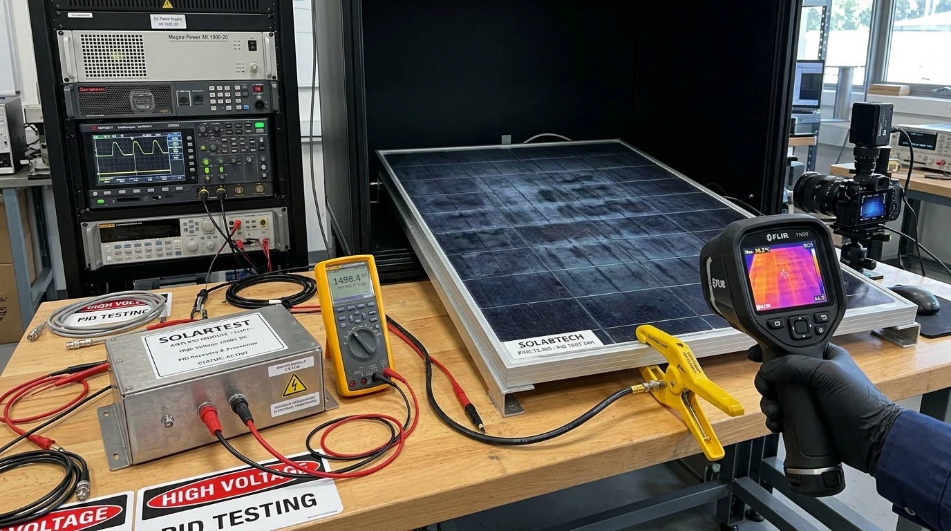
Executive Summary: The Microscopic Quantum Defects of Solar Module Aging
When evaluating photovoltaic modules, system designers and financial analysts rely heavily on manufacturer performance warranties: typically guaranteeing at least ninety-eight percent of nameplate power at the end of the first year, followed by an annual degradation rate between zero-point-four percent and zero-point-seven percent over twenty-five to thirty years.
However, the physical reality inside the silicon wafer is far more dynamic. From the very moment a freshly manufactured solar panel is hoisted onto a rack and struck by photons, invisible quantum reactions begin altering the atomic structure of the semiconductor.
Two primary microscopic mechanisms dictate the early and intermediate lifespan of crystalline silicon cells:
- Light-Induced Degradation (LID): A rapid, photo-activated defect activation that causes immediate power loss—often between one percent and three percent—within hours or days of initial solar deployment.
- Light and Elevated Temperature Induced Degradation (LeTID): A more insidious, thermally driven defect cycle that progresses over months and years in hot field operating environments, capable of eroding an additional three to ten percent of system capacity before stabilizing.
As the solar industry transitions away from legacy p-type Passivated Emitter and Rear Cell (PERC) technology toward next-generation n-type Tunnel Oxide Passivated Contact (TOPCon) and Silicon Heterojunction (HJT) architectures, understanding the physics of these degradation pathways is critical for accurate financial yield modeling, warranty claim substantiation, and component procurement.
Physics of Light-Induced Degradation in Crystalline Silicon
Boron-Oxygen Defect Complex Formation and Carrier Lifetime Collapse
For decades, the dominant substrate for commercial crystalline silicon solar cells was p-type silicon doped with boron. During the standard Czochralski (Cz) crystal-pulling process, molten silicon is contained in high-purity fused quartz crucibles. At temperatures exceeding fourteen hundred degrees Celsius, trace amounts of oxygen dissolve from the crucible walls into the molten silicon ingot, leaving interstitial oxygen atoms () frozen throughout the silicon crystal lattice.
Under dark conditions at room temperature, boron dopant atoms and interstitial oxygen atoms remain separated and electrically benign. However, upon exposure to sunlight:
- Incoming photons generate excess minority charge carriers (electrons in the p-type base).
- The presence of free carriers lowers the activation energy for oxygen dimer diffusion.
- Fast-diffusing oxygen dimers () migrate through the lattice and bind with substitutional boron atoms (), forming a metastable Boron-Oxygen (B-O) defect complex:
This B-O complex acts as an aggressive Shockley-Read-Hall (SRH) recombination center near the middle of the silicon bandgap.
Instead of photo-generated electrons traveling to the front p-n junction to produce external current, they are captured and annihilated at these defect sites. Within forty-eight hours of field illumination, minority carrier lifetime () plummets by fifty to eighty percent, dragging down both open-circuit voltage () and short-circuit current ().
+-----------------------------------------------------------------------------+
|              BORON-OXYGEN LIGHT-INDUCED DEGRADATION CYCLE                   |
+-----------------------------------------------------------------------------+
 Fresh Manufactured Cell (Dark)              Illuminated Field Operation (48 hrs)
┌─────────────────────────────────┐         ┌─────────────────────────────────┐
│ Silicon Crystal Lattice         │         │ Recombination Trap Formation    │
│  [B_s] ... [O_i] ... [O_i]      │  Light  │     [B_s - O_2i] Defect         │
│  Isolated atoms = Benign        │ ───────►│  Electrons captured & lost      │
│  Long carrier lifetime (>200µs) │         │  Carrier lifetime drops (<40µs) │
└─────────────────────────────────┘         └─────────────────────────────────┘
                                                           │
                                        Causes 1.5% to 3.0% Immediate Power Drop
Gallium Doping as a Countermeasure in Monocrystalline Wafers
To combat B-O complex formation without abandoning p-type cell manufacturing lines, tier-one wafer manufacturers transitioned from boron doping to gallium doping in the late 2010s.
Because gallium atoms do not react with interstitial oxygen dimers to form recombination traps, gallium-doped p-type monocrystalline silicon exhibits near-total immunity to classic boron-oxygen LID, reducing initial flash-test degradation to under zero-point-five percent. However, gallium-doped cells remained vulnerable to a secondary, more complex thermal degradation mechanism: LeTID.
Light and Elevated Temperature Induced Degradation Dynamics
Hydrogen Passivation Migration and Thermal Trapping Kinetics
Unlike classic LID, which occurs rapidly at room temperature, Light and Elevated Temperature Induced Degradation (LeTID) requires both solar illumination and elevated cell operating temperatures (typically between fifty degrees Celsius and eighty-five degrees Celsius)—conditions routinely encountered by rooftop arrays and ground mounts throughout the summer months.
The fundamental culprit behind LeTID is hydrogen ().
During the manufacturing of modern passivated solar cells (such as PERC), hydrogen is intentionally introduced by depositing a hydrogen-rich silicon nitride () anti-reflective coating, followed by a rapid high-temperature contact-firing furnace step (). The heat drives atomic hydrogen into the bulk silicon wafer, where it passivates dangling silicon bonds and metal impurity defects, boosting cell efficiency from eighteen percent to over twenty-two percent.
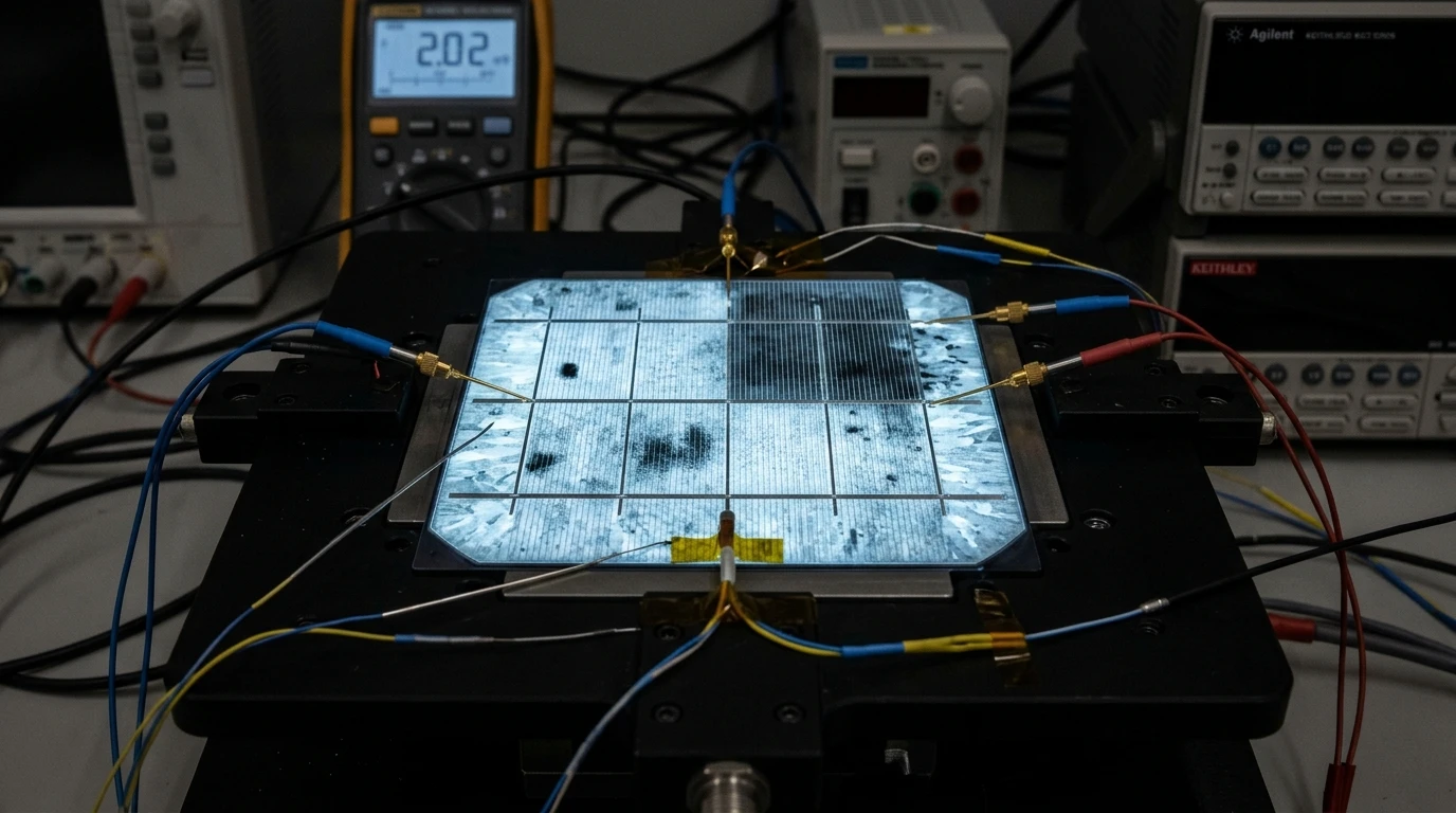
However, this hydrogen is only weakly bonded:
- Defect Activation: Under sustained sunlight and operating temperatures above fifty degrees Celsius, hydrogen atoms dissociate from their passivated sites.
- Defect Complexing: Mobile hydrogen species migrate through the crystal lattice and bind with latent background impurities (such as iron, cobalt, or vacancy clusters), forming highly active deep-level recombination traps.
- Severe Efficiency Slump: Unlike LID, which plateaus within days, LeTID progresses steadily over twelve to thirty-six months of field exposure, causing an additional three percent to ten percent loss in power output.
The Three-Phase Degradation and Regeneration Lifecycle
LeTID is unique among semiconductor degradation mechanisms because it exhibits a characteristic three-phase lifecycle:
- Phase One (Degradation): Power output gradually declines over the first one to two years of field operation as hydrogen dissociates and activates defect complexes.
- Phase Two (Trough): The cell reaches minimum carrier lifetime and lowest power output; the rate of new defect formation balances the rate of defect dissociation.
- Phase Three (Regeneration): Under continued thermal excitation and carrier injection, hydrogen atoms re-configure into stable, electrically inactive molecular complexes () or re-passivate defects permanently. Power output gradually recovers over subsequent years, though rarely returning one hundred percent to initial factory flash-test ratings.
In hot, arid climates (such as the American Southwest, Middle East, or Australia), cells spend thousands of hours per year above sixty degrees Celsius, accelerating both the degradation and regeneration cycles. In temperate or cold climates, cells may remain trapped in the degraded trough phase for up to a decade.
Cell Architecture Comparison: Passivated Emitter Versus Advanced Junctions
Passivated Emitter and Rear Cell Vulnerabilities
Standard p-type PERC cells are intrinsically vulnerable to LeTID due to their thin dielectric passivation layers and heavy reliance on contact-firing hydrogen injection. Because both the front emitter and rear aluminum-alloyed field contain significant defect precursors, un-stabilized PERC modules installed in high-temperature environments routinely suffer severe mid-term power losses that breach standard warranty linear degradation envelopes.
Tunnel Oxide Passivated Contact Immunity Mechanisms
TOPCon (Tunnel Oxide Passivated Contact) technology replaces the p-type silicon base with an n-type silicon wafer doped with phosphorus:
- Zero Boron-Oxygen Complexes: Because the base wafer uses phosphorus instead of boron, classic B-O LID is physically impossible.
- Ultra-Thin Tunnel Oxide: The rear contact consists of an ultra-thin (one to two nanometer) silicon oxide () layer capped with heavily doped polycrystalline silicon. This quantum-mechanical tunnel junction provides extraordinary surface passivation without requiring massive concentrations of unstable mobile hydrogen.
- LeTID Resistance: While early TOPCon variants exhibited minor LeTID susceptibility when firing furnace profiles were improperly tuned, modern n-type TOPCon cells maintain degradation rates below one percent in year one and under zero-point-four percent annually thereafter.

Silicon Heterojunction Intrinsic Layer Passivation Resilience
HJT (Silicon Heterojunction) represents the ultimate technological barrier against photo-thermal degradation:
- Low-Temperature Deposition: HJT cells are manufactured entirely at temperatures below two hundred degrees Celsius using plasma-enhanced chemical vapor deposition (PECVD).
- Absence of Firing Furnaces: Because HJT avoids the seven-hundred-fifty-degree contact-firing furnace required by PERC and TOPCon, hydrogen is deposited within ultra-thin amorphous silicon () intrinsic layers in extremely stable, low-energy configurations.
- Absolute Immunity to LeTID: Extensive accelerated stress testing by national laboratories (NREL, Fraunhofer ISE) confirms that HJT cells exhibit virtually zero measurable LeTID, retaining over ninety percent of rated output after thirty years.
Laboratory Metrology and Diagnostic Techniques
Electroluminescence Imaging and Dark Spot Defect Mapping
In field environments, degraded modules rarely display visible external signs: the front glass, EVA encapsulant, and busbars appear pristine. Identifying microscopic recombination defects requires Electroluminescence (EL) Imaging:
- Forward Bias Injection: In a darkened test chamber or at night in the field, technicians connect a DC power supply to the solar module terminals, driving current in the forward direction (acting like a giant light-emitting diode).
- Near-Infrared Detection: As injected electrons and holes recombine radiatively, they emit near-infrared photons at a wavelength of approximately eleven hundred fifty nanometers.
- Defect Visualization: Sensitive InGaAs or cooled silicon CCD cameras capture this emission:
- High-efficiency, defect-free areas glow with uniform brightness.
- Areas crippled by B-O defects, LeTID recombination traps, micro-cracks, or inactive crystal grains appear as dark grey or jet-black patches.
Photoluminescence and Microwave-Detected Photoconductance Decay
For laboratory-grade semiconductor characterization without physical terminal contacts:
- Photoluminescence (PL) Imaging: High-intensity laser diodes excite carrier generation optically, mapping spatial lifetime distributions across raw silicon wafers before metallization.
- Microwave-Detected Photoconductance Decay (): A pulsed laser flash generates excess carriers, while a microwave probe tracks the decay rate of wafer conductivity. The measured effective carrier lifetime () directly quantifies the concentration of active recombination centers ().
Lifetime Economic Impact and Financial Degradation Modeling
In financial pro-formas for utility-scale and commercial distributed generation, energy yield models (such as PVsyst or SAM) apply annual degradation derate factors. The difference between legacy p-type PERC and modern n-type TOPCon or HJT represents substantial financial value:
For a one-megawatt commercial rooftop array operating in a high-ambient climate:
- p-type PERC (2.0% Year 1 + 0.55%/yr): After twenty-five years, retains approximately eighty-four-point-eight percent nameplate output.
- n-type TOPCon (1.0% Year 1 + 0.40%/yr): After twenty-five years, retains eighty-nine-point-four percent nameplate output.
- n-type HJT (1.0% Year 1 + 0.30%/yr): After twenty-five years, retains ninety-১point-eight percent nameplate output.
This four-to-seven percent higher lifetime generation directly lowers the Levelized Cost of Electricity (LCOE) by eight to twelve dollars per megawatt-hour, overwhelmingly offsetting the marginal initial capital expenditure of n-type hardware.
Comparison: Photovoltaic Cell Architectures and Degradation Rates
The following engineering reference table benchmarks degradation characteristics, defect physics, and warranty protections across crystalline silicon cell technologies:
| Parameter / Metric | p-type Standard PERC | p-type Gallium PERC | n-type TOPCon | n-type Heterojunction (HJT) |
|---|---|---|---|---|
| Wafer Doping Type | Boron-doped p-type | Gallium-doped p-type | Phosphorus-doped n-type | Phosphorus-doped n-type |
| Susceptibility to Classic LID | High (1.5% to 3.0% loss) | Negligible (Under 0.5%) | Zero (Immune) | Zero (Immune) |
| Susceptibility to LeTID | High (3% to 10% in heat) | Moderate (2% to 6%) | Extremely Low (Under 1%) | Zero (Immune) |
| Typical Year One Warranty | 97.5% to 98.0% | 98.0% | 98.5% to 99.0% | 99.0% |
| Annual Linear Degradation | 0.55% to 0.70% / year | 0.45% to 0.55% / year | 0.40% / year | 0.25% to 0.30% / year |
| 30-Year Guaranteed Power | 80.0% to 82.0% | 83.5% to 84.5% | 87.4% to 88.0% | 90.0% to 91.8% |
| Temperature Coefficient | -0.35% / °C | -0.34% / °C | -0.30% / °C | -0.26% / °C |
| Bifaciality Factor | 70% ± 5% | 70% ± 5% | 80% ± 5% | 90% ± 5% |
Engineering Guidelines for Minimizing Array Degradation in the Field
- Prioritize n-Type Silicon for Warm Climates: For any solar installation where module operating temperatures routinely exceed fifty degrees Celsius (rooftop flush-mounts, warm geographic regions, enclosed canopies), mandate n-type TOPCon or HJT modules in procurement specifications to permanently sidestep LeTID degradation troughs.
- Require Certified IEC Testing Standards: Ensure module data sheets certify compliance with IEC TS 63342 (Light and elevated temperature induced degradation testing of crystalline silicon PV modules) and IEC 61215.
- Conduct Pre-Commissioning Baseline Testing: Perform nighttime drone-based Electroluminescence imaging or localized I-V curve tracing on baseline strings during initial system commissioning to document true Day-Zero carrier performance before commercial warranties take effect.
- Optimize Rear-Side Airflow to Lower Cell Temperatures: For rooftop arrays, maintain at least four to six inches of clear stand-off height between roof deck shingles and panel backsheets; lowering peak operating temperatures by ten degrees Celsius dramatically slows thermally activated hydrogen defect migration.